Lesson 8 · Stacking the Deck
Mission: optimize a whole multi-layer stack at once — not just a single
meta-atom. You'll meet the Structure class, build a
two-layer anti-reflection coating with it, plot the result, and then meet the
shared-parameter trick that lets a handful of knobs drive a dozen layers.
Lesson 7 optimized one patterned layer. Real devices stack
them — a disk in one layer, a cross in another, or a graded cone sliced into
sub-layers. A MetaAtom can't express that. A Structure can.
Needs pymoo
pip install "ikarus-rcwa[inverse]".
The idea: declare, then define
You subclass Structure, declare each parameter as a class attribute
(free(...) for a degree of freedom, a plain value for fixed), and implement
define(self, p) to lay out the layers. Inside define, p carries the
resolved values — the optimizer's picks for the free ones — and you call
self.add_layer(...). The cover, substrate and period are added for you.
A two-layer AR coating (the runnable example)
A silicon-nitride disk over a TiO₂ disk on glass — two patterned layers, with both radii, both heights and the period free, all optimized together to minimise reflection at 600 nm. Everything here is a lossless dielectric, so it's fast and R + T = 1 (a clean energy check). Copy-paste the whole thing:
import os
os.environ.setdefault("OMP_NUM_THREADS", "1")        # single-thread BLAS for the GA loop

import numpy as np
import matplotlib.pyplot as plt
from ikarus.inverse import Structure, free, optimize, Target
from ikarus.shapes import Circle


class ARStack(Structure):
    cover, substrate, resolution = "Air", "SiO2", 64
    period = free(0.20e-6, 0.40e-6)     # sub-wavelength pitch (free)
    h1 = free(0.05e-6, 0.30e-6)         # layer-1 height (free)
    h2 = free(0.05e-6, 0.30e-6)         # layer-2 height (free)
    r1 = free(0.10, 0.48)               # disk radius, layer 1 (free)
    r2 = free(0.10, 0.48)               # disk radius, layer 2 (free)

    def define(self, p):
        self.add_layer(p.h1, Circle(radius=p.r1), ["Air", "Si3N4"])   # SiN disk in air
        self.add_layer(p.h2, Circle(radius=p.r2), ["Air", "TiO2"])    # TiO2 disk in air


# 1. optimize (5 DOF, ~30 s with these light settings)
best = optimize(ARStack(), Target.minimize("R", at=600e-9),
                n_orders=6, pop=10, n_gen=6, seed=0)
print(best.report())

# 2. sweep the optimized stack and PLOT it
design = best.rcwa                       # the assembled, ready-to-simulate RCWA
wl = np.linspace(450e-9, 750e-9, 31)
R, T = [], []
for w in wl:
    design.set_source(wavelength=w, theta=0, polarization="linear")
    res = design.simulate()[2]
    R.append(res.R_total)
    T.append(res.T_total)
R, T = np.array(R), np.array(T)

plt.figure(figsize=(7, 4))
plt.plot(wl * 1e9, R * 100, lw=2, label="Reflectance")
plt.plot(wl * 1e9, T * 100, lw=2, label="Transmittance")
plt.plot(wl * 1e9, (R + T) * 100, "--", lw=1, label="R + T")   # ≈ 100%: lossless → energy conserved
plt.xlabel("wavelength (nm)"); plt.ylabel("efficiency (%)")
plt.title("Two-layer dielectric AR stack (optimized)")
plt.ylim(0, 105); plt.legend(); plt.grid(alpha=0.3)
plt.tight_layout()
plt.savefig("ar_stack_spectrum.png", dpi=150, bbox_inches="tight")

# 3. (optional) see the optimized layers
design.visualize_structure(plane="xy", layer_index=1, savefig="ar_layer1.png")  # SiN disk
design.visualize_structure(plane="xy", layer_index=2, savefig="ar_layer2.png")  # TiO2 disk
plt.show()
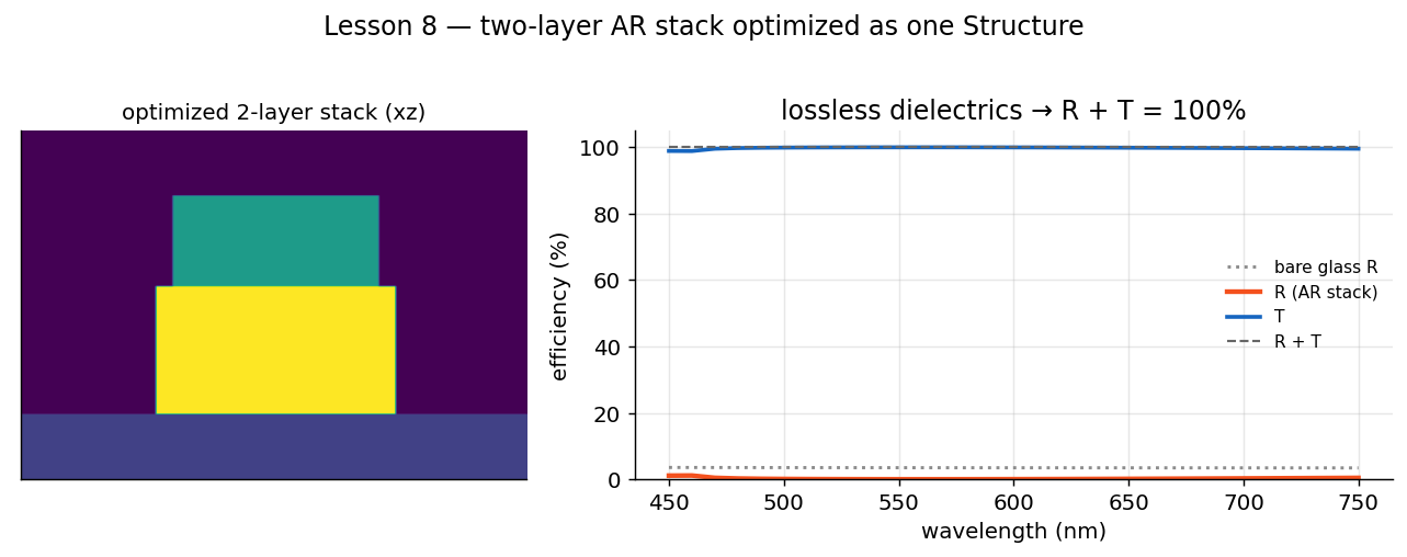
That R + T = 100% line is worth dwelling on: for lossless materials, energy
is conserved, so it should sit at 100% at every wavelength. If it doesn't, either
you're under-converged (raise n_orders) or a material absorbs — which is exactly
what happens next.
Shared / derived parameters (advanced)
Here's the thing no single-layer construct can do: drive many layers from a few parameters. A moth-eye is a graded cone — RCWA models it as a stack of slices whose radii are all functions of two numbers, so four DOF describe the whole cone:
from ikarus.inverse import Structure, free, optimize, Target
from ikarus.shapes import Circle

class MothEye(Structure):
    cover, substrate, resolution = "Air", "Si", 96
    N = 12                                  # slices (fixed)
    period = free(150e-9, 240e-9)
    height = free(200e-9, 1000e-9)
    r_base = free(0.15, 0.5)
    gamma  = free(0.5, 3.0)

    def define(self, p):
        for i in range(p.N):
            r = p.r_base * ((i + 0.5) / p.N) ** p.gamma     # every slice from r_base & gamma
            self.add_layer(p.height / p.N, Circle(radius=r), ["Air", "Si"])
This example is deliberately a hard problem — expect it to be slow
A broadband moth-eye on silicon is about the worst-case problem for RCWA,
and it's here to show off Structure, not because RCWA is the right tool:
- It's slow. Each evaluation solves a 12-layer stack across several
wavelengths; a full
optimize(...)run can take tens of minutes. The progress bar will sit on one generation for minutes at a time — it has not crashed. (For real broadband 3-D work, a volumetric solver like FDTD is the better choice.) - R + T ≠ 1 here, and that's correct. Silicon is strongly absorbing across 300–600 nm (n = 5 + 4.2 i at 300 nm!), so most of the light is absorbed, not transmitted. That's the whole point of a "black-silicon" moth-eye — you minimise reflection so light couples into the silicon and gets absorbed. So optimise and plot R only:
best = optimize(MothEye(),
                Target.minimize("R", band=(300e-9, 600e-9, 6), worst_case=True),
                n_orders=8, pop=10, n_gen=6, seed=0, progress=True)   # minutes!
print(best.report())

import numpy as np, matplotlib.pyplot as plt
design = best.rcwa
wl = np.linspace(300e-9, 600e-9, 31)
R = []
for w in wl:
    design.set_source(wavelength=w, theta=0, polarization="linear")
    R.append(design.simulate()[2].R_total)        # reflectance is the metric here
plt.plot(wl * 1e9, np.array(R) * 100)
plt.xlabel("wavelength (nm)"); plt.ylabel("reflectance (%)"); plt.show()
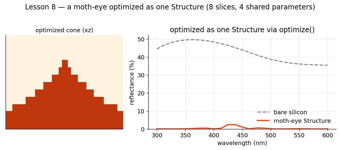
Structure — twelve slices driven by four shared parameters. Left: the cone (xz). Right: reflectance vs. bare silicon (R only — the substrate absorbs).The point isn't the runtime — it's that four shared parameters drove twelve
layers, expressed in three lines of define(). That's the capability; reach for
it on problems RCWA is actually fast at (thin dielectric stacks, gratings,
metasurfaces), and it shines.
How it plugs in
optimize() doesn't care whether you hand it a MetaAtom or a Structure — it
only calls two methods on the design:
variables()→ the free DOF (auto-discovered from yourfree(...)attributes),build(params, n_orders)→ the assembledRCWA.
Structure implements both from your define(). (So could a class of your own —
see the decision guide.)
Pilot habits
- Always declare a
period(free or fixed) —Structurerequires it. - Watch
R + T. For lossless dielectrics it must be ≈ 100%; a shortfall means absorption (fine, if intended) or under-convergence (raisen_orders). - Keep DOF physical and few: shared/derived parameters (the cone's
r_base,gamma) converge far faster — and stay manufacturable. - Optimize at a light
n_ordersfor speed, then confirm the winner at a higher one (the convergence ritual). - Match the tool to the job: RCWA is fast for thin layered dielectrics, slow for thick high-index 3-D broadband problems.
🎓 Flight School complete — all eight lessons flown. Where to next: Aerobatics · The Hangar · Inverse Design API